EN
EN  EN
EN DA
DA NL
NL FI
FI FR
FR DE
DE IT
IT JA
JA KO
KO NO
NO PL
PL PT
PT RO
RO RU
RU ES
ES SV
SV TL
TL ID
ID SK
SK UK
UK VI
VI TH
TH TR
TR FA
FA BE
BE LA
LA UZ
UZ
Abstract:
As the core material of next-generation power semiconductors, silicon carbide (SiC) is driving significant improvements in energy efficiency and system performance. In the SiC device manufacturing chain, silicon carbide epitaxy is a decisive step in laying the foundation for device performance. This article will explore in depth the definition of SiC epitaxy, key equipment for the epitaxy process, its specific applications in semiconductor processing, and the problems and challenges it faces.
Definition of SiC Epitaxy
Silicon carbide epitaxy is a crystal growth technique that involves the growth of one or more layers of a single crystal silicon carbide film (i.e., epilayer) with a specific crystallographic orientation (usually the same as that of the substrate) on a single-crystal silicon carbide substrate (SiC Substrate) that has been cut and polished, by means of Chemical Vapor Deposition (CVD), etc. The epilayer is a thin film of very high quality with a precisely controlled doping concentration and thickness. The process of growing one or more layers of single-crystal silicon carbide (epilayer) on a SiC substrate by chemical vapor deposition (CVD) or other methods, with a specific crystal orientation (usually the same as the substrate), very high quality and precisely controlled doping concentration and thickness.
The core objectives are:
● To provide a functional layer with low defects: the epilayer has a lower density of crystal defects compared to the substrate material.
● Precise control of electrical properties: The ability to precisely control the doping type (N- or P-type), doping concentration (in the range of 1014 to 1019 cm-3), and thickness (from a few micrometers to hundreds of micrometers) of the epilayer.
● Building Device Structure: Provide the basic platform for fabricating the active regions (e.g., drift layer, channel region, body region, etc.) of the device for the subsequent ion implantation, photolithography, etching, metallization, and other processes.
SiC Epitaxy Equipment and the Applications
The core equipment for performing SiC epitaxy processes are high temperature chemical vapor deposition (HTCVD) reactors. These are highly complex systems designed for precise control of crystal growth under extreme conditions (high temperatures, specific atmospheres).
Equipment Types and Features:
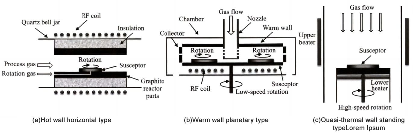
Three kinds of silicon carbide epitaxial growth furnace and core accessories differences
1)Mainstream Technology: Hot-wall CVD is widely used in industry today. This design makes the temperature distribution in the reaction chamber more uniform, which is conducive to improving the thickness of the epitaxial layer and doping uniformity.
2)Heating method: Induction heating or resistive heating is commonly used to achieve the ultra-high temperatures required for SiC epitaxy (typically >1500°C, even up to 1600-1700°C).
3)Reaction chamber configurations:
● Horizontal Reactors: Gas flows horizontally through a wafer placed on a graphite base (Susceptor). Relatively simple structure, but large size uniformity control is a challenge.
● Planetary/Vertical Rotating Reactors: Wafers are placed on rotating pedestals, usually with multiple satellite pedestals rotating simultaneously around a center. This design significantly improves the temperature and airflow uniformity of large wafers through rotation and revolution and is currently the dominant equipment choice for high volume production, especially for 150mm and 200mm wafers. Representative equipment manufacturers such as LPE, Aixtron, etc. provide such equipment.

LPE Halfmoon SiC EPI Reactor
4)Gas Transportation Systems:
Need to precisely control the flow of a variety of gases, including:
● Precursors: Silicon sources (e.g., silane SiH4), carbon sources (e.g., propane C3H8 or ethylene C2H4), and carbon sources (e.g., ethylene C2H4). H4).
● Carrier Gas: usually high purity hydrogen (H2), sometimes mixed with argon (Ar).
● Dopants: Nitrogen (N2) for N-type doping; trimethylaluminum (TMA) or ethylborane (B2H6) for P-type doping.
● Etching gases: e.g. hydrogen chloride (HCl) for chamber cleaning or in-situ etching.
5)Automation and Control:
The equipment needs to be equipped with an advanced control system to monitor and regulate parameters such as temperature, pressure, gas flow, base speed, etc. in real time to ensure process stability and repeatability.
Applications in Semiconductor Processing:
1) Production of SiC Epi-wafers: The immediate output of a CVD reactor is SiC wafers with high quality epitaxial layers. This is the starting point for all subsequent SiC device manufacturing.
2) Fabrication of Power Devices: These epi-wafers are sent to a chip fabrication facility (Fab) for the production of:
● SiC MOSFETs: The devices need to accurately grow multilayered structures such as N- drifts, P-bodies/wells, etc., and the quality of the epitaxial layer has a direct impact on the Rds(on), Threshold Voltage (Vth), Breakdown Voltage (Vth), and the RDS(on) of the device. ), breakdown voltage (Vbr) and reliability.
● SiC SBDs: The equipment is mainly used to grow the N- drift layer, which determines the reverse blocking capability and forward voltage drop of the diode.
3) Supporting R&D activities: Epitaxy equipment is also used to develop new epitaxial processes, explore new material properties and develop novel device structures.
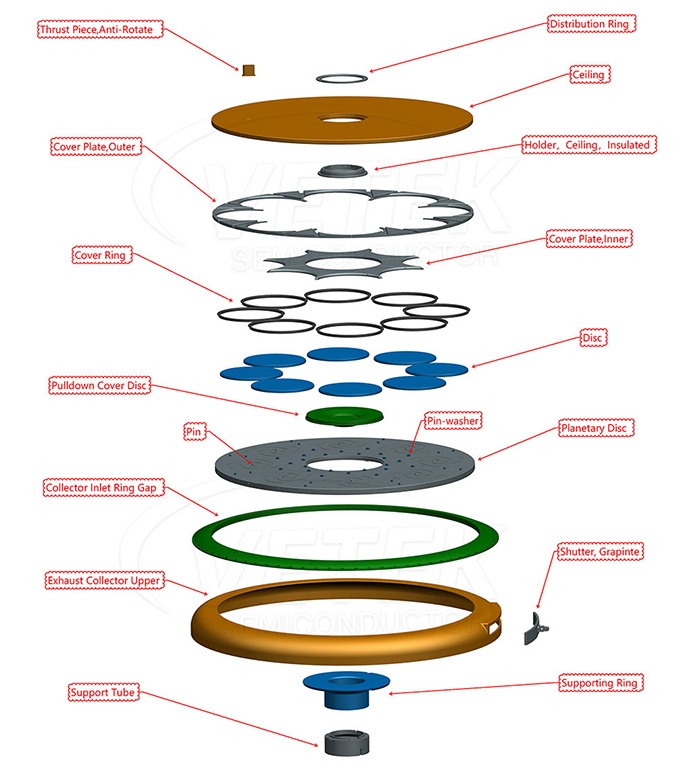
List of Aixtron Planetary Reactor parts
Problems and Challenges of SiC Epitaxy Equipment and Processes in Applications
The high complexity of SiC epitaxy equipment and the extreme conditions of the process make it face a number of serious challenges in practical applications:
Challenges at the equipment level
● Temperature uniformity and control: At temperatures >1500°C, it is extremely challenging to achieve accurate temperature control within a few degrees Celsius across a large footprint (carrying 150mm or 200mm wafers). Small deviations in temperature can lead to uneven epitaxial layer thickness and doping concentration.
● Gas flow design and optimization: The gas flow pattern in the reaction chamber is critical to growth rate and uniformity. Equipment design requires complex hydrodynamic simulations and experiments to optimize the showerhead, chamber geometry, and airflow parameters to avoid vortices, dead zones, and gas-phase nucleation (particle generation).
● Equipment Stability and Maintenance: High temperatures and corrosive gases (e.g., HCl) cause severe wear and tear on chamber internals (e.g., graphite, quartz). High-temperature and corrosion-resistant materials with regular maintenance and part replacement are required to ensure process window stability and low particle contamination. This increases operating costs and downtime.
● Particle Control: Tiny particles generated inside the device are one of the main causes of epitaxial layer surface defects and device failure. Extremely clean air sources, precision filters, and optimized chamber cleaning procedures are required.
● Equipment cost and capacity: SiC epitaxy equipment is inherently expensive. At the same time, growth rates are often limited to ensure high quality, especially for thick epitaxial layers, and the capacity (Wafers Per Hour (WPH)) of a single unit is relatively limited, which directly affects the cost of SiC epitaxial wafers. Planetary reactors have higher capacity, but are more complex and costly.
● Transition to 200mm wafers: Scaling existing mature 150mm process and equipment designs to 200mm wafers presents significant challenges, especially in maintaining or even improving uniformity and defect control.
Process Level Challenges (closely related to equipment)
● Defect control: How to effectively suppress or eliminate dislocations (TSD, TED) extending from the substrate, as well as surface defects (craters, scratches, step aggregates) and internal defects (stacking errors) generated during epitaxy is a constant challenge. Optimization of equipment parameters (temperature, pressure, C/Si ratio, growth rate) is critical.
● Thick film epitaxy: High voltage devices require low doped epitaxial layers tens or even hundreds of microns thick. Maintaining low defect density, high uniformity, and stable growth rates over such long growth times is difficult.
● Doping control: Achieving highly consistent doping concentrations (especially low doping in the 1014-1015cm-3 range) across large wafer sizes and from batch to batch, as well as steeply doped interfaces, requires equipment with very high stability and precise gas flow control. low activation efficiencies and memory effects of P-type doping (Al) are also challenges. memory effects are also challenges.
Founded in 2018, Semixlab Technology Co.,Ltd is a technology-based enterprise focusing on the research and development, production and sales of advanced materials. It is a world-leading semiconductor material manufacturer.