EN
EN  EN
EN DA
DA NL
NL FI
FI FR
FR DE
DE IT
IT JA
JA KO
KO NO
NO PL
PL PT
PT RO
RO RU
RU ES
ES SV
SV TL
TL ID
ID SK
SK UK
UK VI
VI TH
TH TR
TR FA
FA BE
BE LA
LA UZ
UZ
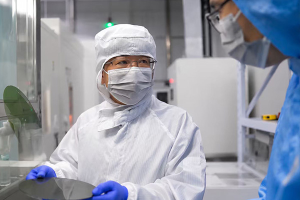
In semiconductor manufacturing even very small particles or alignment errors can lead to serious problems like lower yields and expensive downtime. Because of this the equipment used to move wafers must be extremely precise and clean. SiC ceramic robotic arms are becoming popular because they are strong stable and resistant to heat and chemicals while producing very few particles. Unlike metal or plastic arms they can handle repeated high temperature processes without bending or releasing contaminants. For engineers and fab operators this means wafers are handled more safely processes stay consistent and production runs more smoothly overall.
Why SiC Ceramics Are Ideal for High-Precision Wafer Handling
Handling wafers in a semiconductor fab is an extremely delicate process because each wafer is thin fragile and coated with layers that can be easily damaged. Even a small mistake in movement or positioning can create defects that reduce yields. This is where SiC ceramic robotic arms really stand out. Made from silicon carbide, these arms are incredibly hard and remain stable even under high temperatures, so they don't warp or expand like metal arms might. This stability allows wafers to be held and moved with consistent accuracy during demanding processes such as epitaxy or etching. SiC is also highly resistant to chemicals, which is important because wafers often pass through chambers with reactive gases or plasma. Unlike traditional metals that can corrode or release particles, SiC stays inert and helps maintain a cleaner environment, reducing the risk of contamination that could ruin advanced chips. The material's light weight also allows motors and actuators to work more efficiently, improving response times and reducing vibrations, which makes precise placement easier and more reliable over thousands of wafer movements. Real-world results back this up: in one 200mm fab, switching from metal to SiC arms cut wafer breakage in half and noticeably reduced particle-related defects, while maintenance became less frequent thanks to the material's durability under repeated high-temperature cycles. For engineers and fab operators who prioritize precision cleanliness and reliability, SiC ceramic arms offer a solution that combines performance and durability, keeping wafers safe and processes consistent without adding extra risk.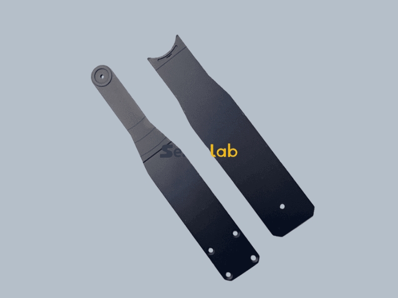
How SiC Eliminates Particle Generation Compared to Traditional Materials
Particle contamination is a major challenge in semiconductor fabs because even tiny dust, metal, or debris can stick to wafers and cause defects, especially as chip features shrink to the nanometer scale. Traditional robotic arms made of metal or plastic can worsen the problem. Metal arms may wear over time, producing microscopic flakes, while plastics can degrade under high heat or exposure to reactive gases, releasing particles into the cleanroom. SiC ceramic arms solve this issue differently. Silicon carbide is extremely hard and chemically stable, so it doesn't wear down easily and won't shed particles under high temperatures, plasma, or harsh chemicals. Its smooth, inert surface allows wafers to glide without picking up contamination, which is crucial for advanced processes to maintain yield and avoid costly rework. The manufacturing of SiC arms also matters. Precision sintering and machining produce a dense, uniform structure with minimal surface defects, making the arms easier to clean and less prone to trapping dust. Fabs that switch to SiC arms often see particle counts drop, wafer defects decrease, and cleaning cycles extend without risk. In high volume production, this means fewer interruptions, less downtime, and more consistent wafer quality. For engineers focused on keeping wafers pristine, SiC ceramic arms provide a reliable way to move materials safely while minimizing invisible contamination risks.
Founded in 2018, Semixlab Technology Co.,Ltd is a technology-based enterprise focusing on the research and development, production and sales of advanced materials. It is a world-leading semiconductor material manufacturer.